Hardware
Kit Contents
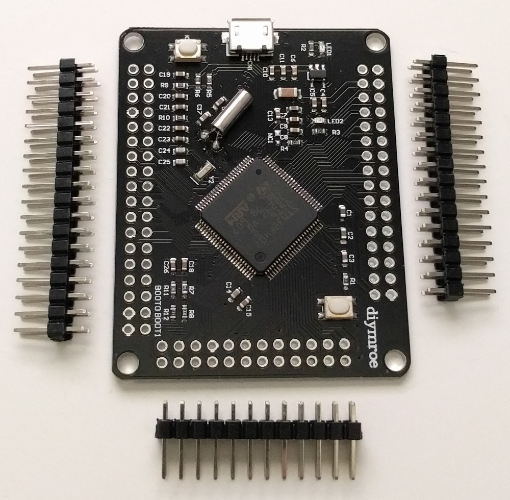
- 1 x STM32F407 Dev Board (male pin header included)
- 1 x ST-LINK V2 STM32 USB Debug Adapter
- 1 x 7-pin SPI 128x64 0.96 inch SSD1306 driven OLED Display Module
- 1 x USB Cable Type A Plug/Male to Type Micro-B Plug/Male
- Female to female jumper wires with 0.1" header contacts
- 2 x 2.54mm pitch jumpers (optional)
About the Kit
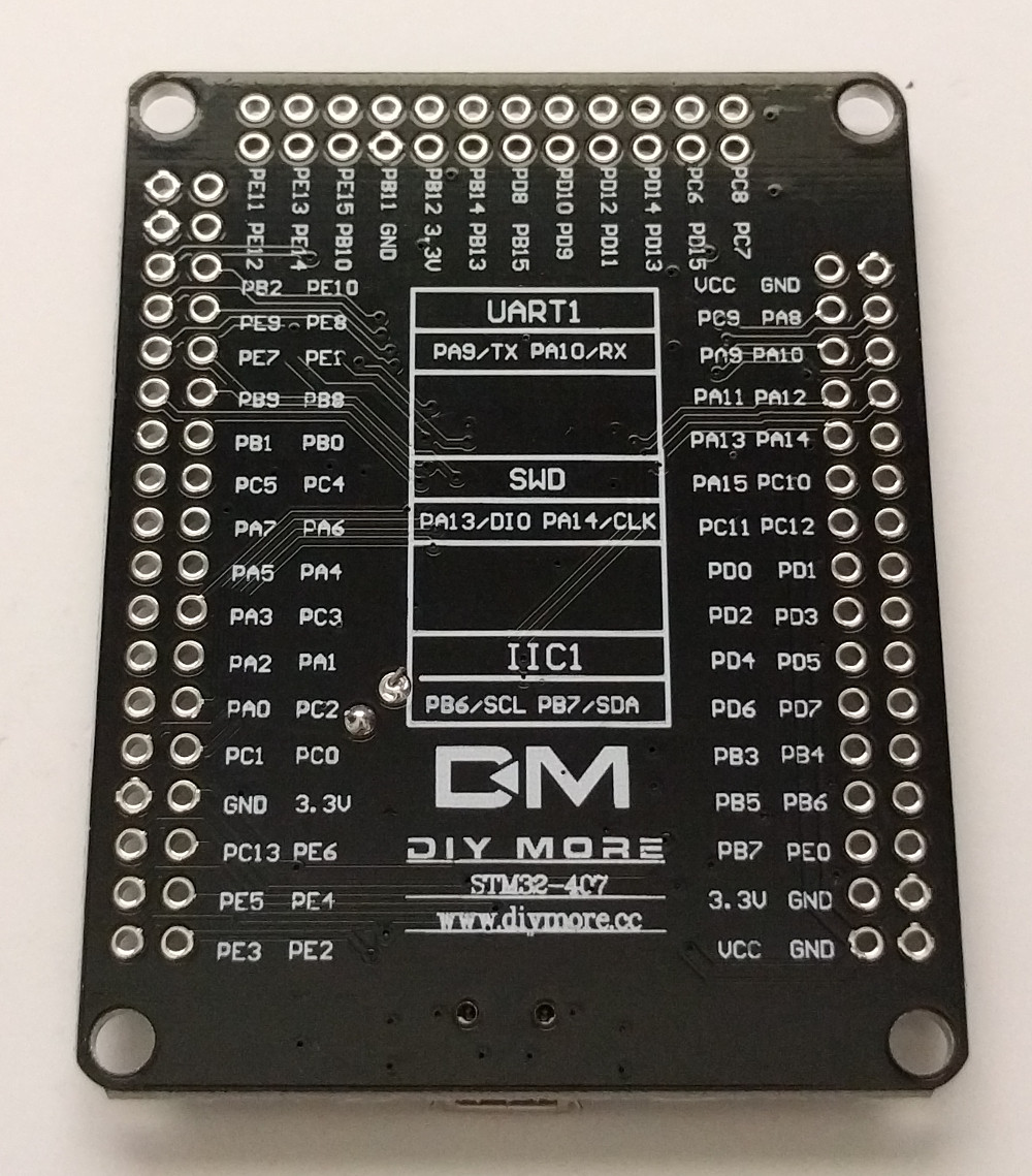
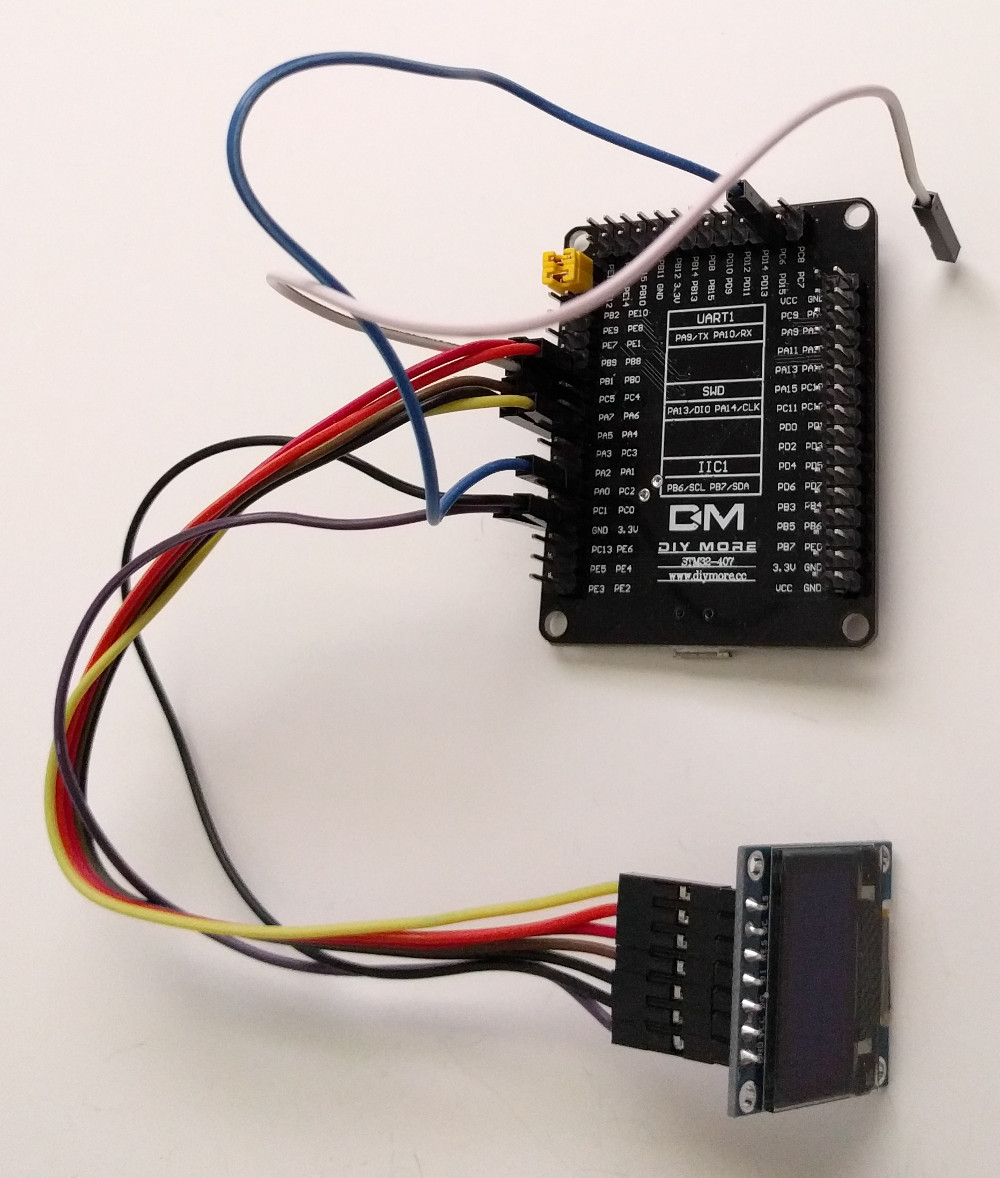
The primary difference between this kit and the other TREZOR One Dev Kits is the low cost dev board used. This kit is also more bare-bones since it relies on (un)attaching a jumper wire to simulate one of the user push buttons. The dev board has one user push button (one the opposite side of the board from the USB connector) and one system reset push button (adjacent to the USB connector). A normal TREZOR One device has two user push buttons and no reset push button. The second user push button (that is mostly used as a "cancel" option) is sacrificed because it is not crucial for most uses. If you get into a case where you need to cancel, you can just unplug the device or use the system reset push button. One function that requires both user push buttons is the boot into firmware update mode. In this case, wire the pin for the second user button (PC5) to GND/ground. Both user push buttons are active-low. That is why wiring to GND works to simulate pressing the button. Also, the user push button is connected to PD15 on the dev board. Connect the pin for user push button 1 (PC2) to pin PD15 with a jumper wire so that you can use the button without changing the software. The two yellow things on the BOOT pins in the pictures are jumpers that connect the BOOT0 and BOOT1 pins to GND. They are just a nicety to reduce the number of wires hanging around. Two female to female jumper wires may be used instead. As can be seen in the pictures, you may solder the pin header to either side of the dev board.
One key difference between this kit and production hardware is the microcontroller (MCU) used. Production hardware uses the STM32F205RET6 (and more recently, the STM32F205RGT6) MCU and these kits use the STM32F407VGT6 MCU. Note: the STM32F205RET6 is documented to have 512KB of flash memory, but it actually has 1MB. Apparently, it is more cost efficient for ST to not develop different chip-wafers. The former is an ARM® Cortex®-M3 and the latter is an ARM® Cortex®-M4. The Cortex-M4 architecture is a backwards compatible superset of Cortex-M3. The additional features, like hard float capability, do not matter for this project. The STM32F407VGT6 has 1MB of flash memory, a core clock frequency adjustable up to 168MHz (including the 205's 120MHz; with matching clock tree), and 128KB of SRAM (same as the 205; the 407 has an additional 64KB of CCMRAM, giving it 192KB of usable RAM). The STM32F407VGT6 is pin-to-pin compatible with the STM32F205RET6/STM32F205RGT6 and uses the same TRNG (reference: STM32F407xx datasheet section 2.1, and AN4230 section 1.2.1).
The dev board has an 8MHz high-speed external (HSE) crystal (matching the reference hardware), a STM32F407VGT6 MCU, a USB connector, a user push button, a reset push button, power circuitry, SWD debug interface, boot mode select pins, and all the pins needed, broken out and available for use.
Setup
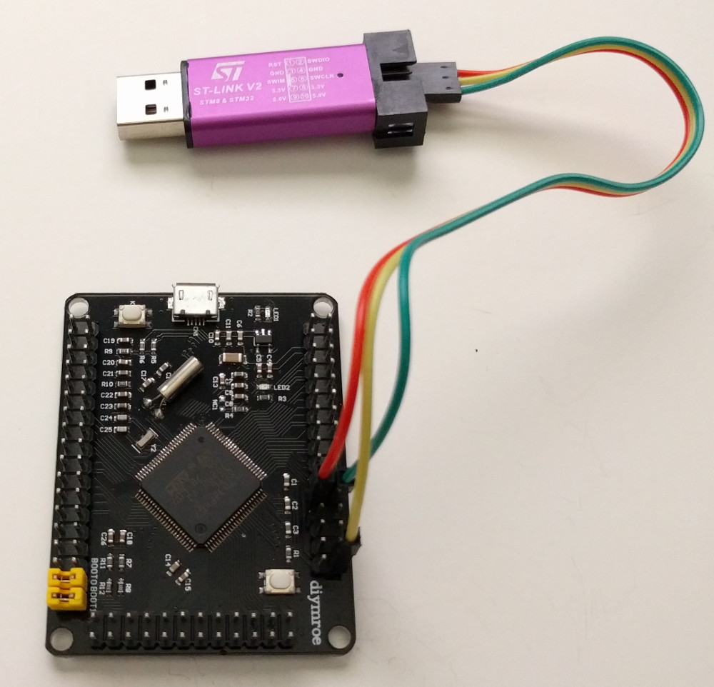
Wiring the Debug Adapter to the Dev Board
Connect the debug adapter's SWDIO, SWCLK, and GND pins to the dev board's PA13, PA14, and GND pins, respectively.
Setting Dev Board Jumpers and Switches
Connect the BOOT0 and BOOT1 pins to GND. See the two yellow jumpers in the pictures. If left disconnected, the BOOT0 and BOOT1 pins will be pulled high. Sometimes this is useful for accessing the DFU bootloader, or to boot from SRAM instead of flash memory.
Wiring the Dev Board to the Breadboard Display and Switches
Pins on the dev board are documented by the silkscreen. Pins on the display module are also documented by silkscreen.
| Dev Board Pin | Breadboard Pin | Alternate Name | Comment |
|---|---|---|---|
| PC5 | Button 2 | Connect jumper wire to pin and leave the other side until needed. When necessary, attach and unattach to GND to simulate pressing and releasing the button; button is Active-Low | |
| PA4 | CS | Chip Select | Pin 7 on Pictured Display |
| PB0 | DC | Data/Command | Pin 6 on Pictured Display |
| PB1 | RES | Reset | Pin 5 on Pictured Display |
| PA7 | SDA | MOSI | Pin 4 on Pictured Display |
| PA5 | SCK | SCLK | Pin 3 on Pictured Display |
| 3.3V | VDD | 3V3 | Pin 2 on Pictured Display |
| GND | GND | Ground | Pin 1 on Pictured Display |
| PC2 | Button 1 | Connect jumper wire from PC2 to PD15; button is Active-Low |